IntelliSense’s IntelliSuite connects layout, virtual fabrication, multiphysics analysis, system modelling and 3D packaging, so engineering teams find problems on screen instead of in the cleanroom.
A technology overview by WaldyTech, IntelliSense’s representative in Israel
Executive Summary
IntelliSuite is a complete design and simulation platform for MEMS, semiconductor processes and advanced packaging, developed by IntelliSense Software Corporation (USA, founded 1991) and used in more than 35 countries. It covers the whole development chain in one environment: mask layout, process simulation, coupled multiphysics analysis, system-level modelling with IC co-simulation, and 3D package design.
Who it is for
- MEMS developers: gyroscopes, accelerometers, pressure sensors, micromirrors, RF MEMS, resonators, microfluidics.
- Process and fab engineers who need to predict etch, deposition and implant results before committing wafers.
- Advanced packaging teams working on chiplets, TSV/TGV interposers, RDL, bumps and system-in-package.
- Defence, aerospace and navigation programmes, where sensor performance over temperature and package stress is critical.
- Photonics, quantum and research groups, including VCSELs, quartz and sapphire devices, diamond NV centres, and universities.
Main strengths
- One connected workflow: design, process, device, system and package share a single model.
- Physics-based process simulation, validated against real SEM cross-sections of silicon, quartz, sapphire, III-V and metals.
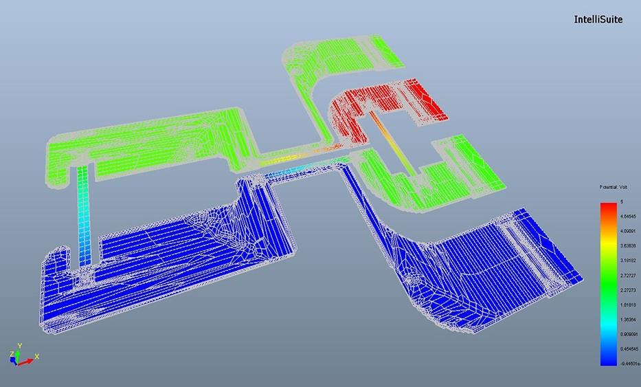
- Fully coupled multiphysics: thermal, electrostatic, mechanical, piezoelectric, piezoresistive, fluidic and electromagnetic.
- MEMS–IC co-simulation through compact macromodels and Verilog-A export.
- Fast and open: GPU-accelerated process simulation, automatic parametric sweeps, and GDSII/DXF and STEP/STL export to third-party tools.
What Sets IntelliSuite Apart
Most MEMS teams work with one of three tool setups: a general-purpose multiphysics simulator, an IC layout tool adapted for MEMS, or several separate tools for layout, process and analysis. Each has its strengths, but each also leaves gaps that IntelliSuite was built to close.
| Typical approach |
Where it falls short for MEMS |
The IntelliSuite approach |
| General-purpose multiphysics simulators |
They analyse idealised CAD geometry that the engineer draws by hand, so real fabrication effects (sloped sidewalls, undercut, corner rounding) are missing. They rely on a single solver method for every physics domain, which makes electrostatic models heavy and slow. |
Analyses the geometry that the process actually produces. The Fastfield solvers use the best method for each domain (for example, boundary elements for electrostatics, finite elements for mechanics and heat), with fewer meshes and faster coupled solutions. |
| IC layout tools used for MEMS |
They are built for Manhattan geometry and electrical design rules. Curved and all-angle MEMS structures are cumbersome, and the layout has no link to process or 3D analysis. |
Blueprint is a layout editor designed for MEMS, with all-angle support, MEMS design rule checks and cross-section views. Masks link directly to process simulation and to one-click meshing. |
| Geometric process emulators |
They extrude and subtract shapes by rule. This is quick, but it cannot predict anisotropic etch fronts, crystal-orientation effects or the influence of temperature and concentration. |
Physics-based etch, deposition, oxidation and implant models with material databases, checked against SEM measurements of fabricated devices. |
| A chain of separate single-purpose tools |
Geometry is re-drawn at each handoff, which introduces errors and delays. Design, process and packaging teams each work on their own model. |
One environment and one model, from schematic to layout, process, device, system and package. Results can still be exported (STEP/STL, Verilog-A) for final sign-off in downstream tools. |
The practical result is fewer fabrication iterations. Design errors that would normally appear only after a wafer run, such as the wrong etch profile, an unexpected frequency shift after packaging or a stress hot spot around a bump, are found in software instead.
IntelliSuite in Practice
Virtual fabrication that matches the lab
Wet anisotropic etching is notoriously hard to predict, and many companies still rely on trial and error. IntelliSuite’s process tools (IntelliFAB and FabSim) simulate it physically, taking crystal orientation, etchant, temperature and time into account. In the sapphire example below, simulated sidewall angles of 146.5° / 119.6° and 132° / 132° closely match the 145° / 121° and 130° / 130° measured by SEM on the fabricated wafer. Dedicated etch-rate databases cover silicon, quartz (Z-cut, AT-cut), sapphire, III-V semiconductors and metals, and GPU acceleration speeds up high-resolution process runs by up to 20 times.
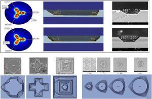
Sapphire (Al₂O₃) wet etching: etch-rate distribution, simulated profile and SEM cross-section of the real device.
Inertial MEMS: a gyroscope, including its package
Gyroscope performance depends on matching the drive and sense modes, controlling quadrature error, and knowing how the package and temperature shift those frequencies. IntelliSuite builds the gyro as a 3D model, calculates its modes, and extracts a compact macromodel for system-level simulation of the Coriolis and quadrature forces. The gyro is then modelled together with its package, predicting the frequency shift from −40 °C to +125 °C before any hardware is built. The same macromodel connects to the readout circuit for full MEMS–IC co-simulation.
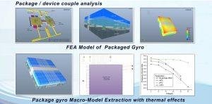
Packaged gyro macromodel with thermal effects: mode frequency versus voltage at −40 °C, 25 °C and 125 °C.
Parametric design, from layout to results automatically
The Designer Control Center runs automatic parameter sweeps. For each variant it generates the layout, builds and meshes the model, runs the analysis and plots the result, with no manual rework. IntelliSense has used this approach on micromirror arrays for space telescopes. A senior scientist at NASA Goddard Space Flight Center noted that IntelliSuite helped identify optimal electrode configurations and reduce fabrication trial and error.
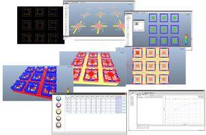
Parametric design of a micromirror array, from layout to automated sweeps.
3D packaging and chiplets
With chiplets, interposers and heterogeneous integration, the package itself becomes a major engineering risk. IntelliSuite’s 3D Packaging & Chiplet Design Suite takes a package from architecture and layout (with interconnect and DRC checks) through the packaging process flow (RDL, UBM, bumps, bonding and underfill) to thermal and stress analysis on the real process-derived structure, before any sample is built.
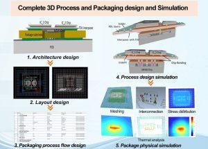
Complete 3D process and packaging design and simulation on a MEMS + IC package.
Emerging devices: photonics and quantum sensing
The same process-aware approach now extends to new device classes. For VCSEL lasers, IntelliSuite models the anisotropic wet oxidation that defines the laser aperture. For diamond NV centres, a leading platform for quantum sensing, it links nitrogen implant energy, dose and anneal temperature to implant depth and NV yield, so process windows can be screened in software instead of on the implanter.
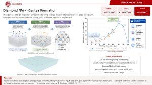
Diamond NV(−) centre formation: process steps, modelled NV array and simulated yield trend.
Looking Ahead
IntelliSense’s development directions include atomic-level process simulation, panel-level and heterogeneous packaging, photonic device workflows, and AI-assisted parameter optimisation that complements physics-based simulation rather than replacing it.
Roadmap items reflect IntelliSense’s development directions as of August 2026 and are not a feature commitment or release schedule.
IntelliSuite in Israel
WaldyTech is IntelliSense’s representative in Israel. With over 20 years of experience supporting Israeli defence, aerospace, industry and research organisations with advanced precision technologies, we help engineering teams evaluate IntelliSuite on their own devices and processes.
Want to see IntelliSuite on your application? Contact WaldyTech for more details.